Can you “vibe code” an FPGA into an I2S FIFO reclocker?

Programming an FPGA is considered top-level DIY digital audio stuff.

You get to implement FIFOs that buffer the audio and get rid of jitter and also implement custom digital filters with performance way beyond what is available on commercial DAC chips.

There is only one catch but it’s a big one.

You have to learn how to program in Verilog or VHDL, which are Hardware Description Languages. So their logic is very different to classic programming languages or even microcontroller programming languages.

If you are doing this as a hobby, and are of a certain age, that may look like a very steep learning curve.

That is precisely why, even though I bought a Spartan 6 development kit almost 10 years ago, I never quite got around to playing with it.

Fast forward to 2026, when AI is now considered a “kindda mature” technology.

All the kids are doing “Vibe coding”, meaning they just discuss with the AIs what they want to implement and then let the AIs do all of the actual programming.
After a few iterations of this process they usually end up with something that functions. It may not be elegant, it may not be optimized, it may not be secure, but at least it functions.
The fact that a non-programmer can create functional (and presumably useful) software is pretty much amazing (ok, a “friggin’ miracle” may be more accurate).

So I thought, what if I could apply this technique to an FPGA design?

So I got to work, and when I say work I mean chatting with Gemini Pro 3.1. So, easy work.

Before I continue, one side note. Not all AIs have the same capabilities. If you think you can accomplish something like this using the “free / fast” models you are sadly mistaken. You will need all the processing power that you can get. I got by with the basic Gemini Pro subscription (~20$ / month) but access to hi-end Claude models would have saved me a lot of time. Not a huge problem for a hobby-grade project, but still..

Now, back to our story.

After I got Gemini’s confirmation that it can indeed do most of the Verilog programming for me, and realizing that the Spartan 6 is pretty much outdated, I set out to pick a suitable FPGA.

The main requirement was that it be “human-solderable”. I should be able to solder it on to a PCB without having to actually manufacture the populated board. That meant no BGA stuff.

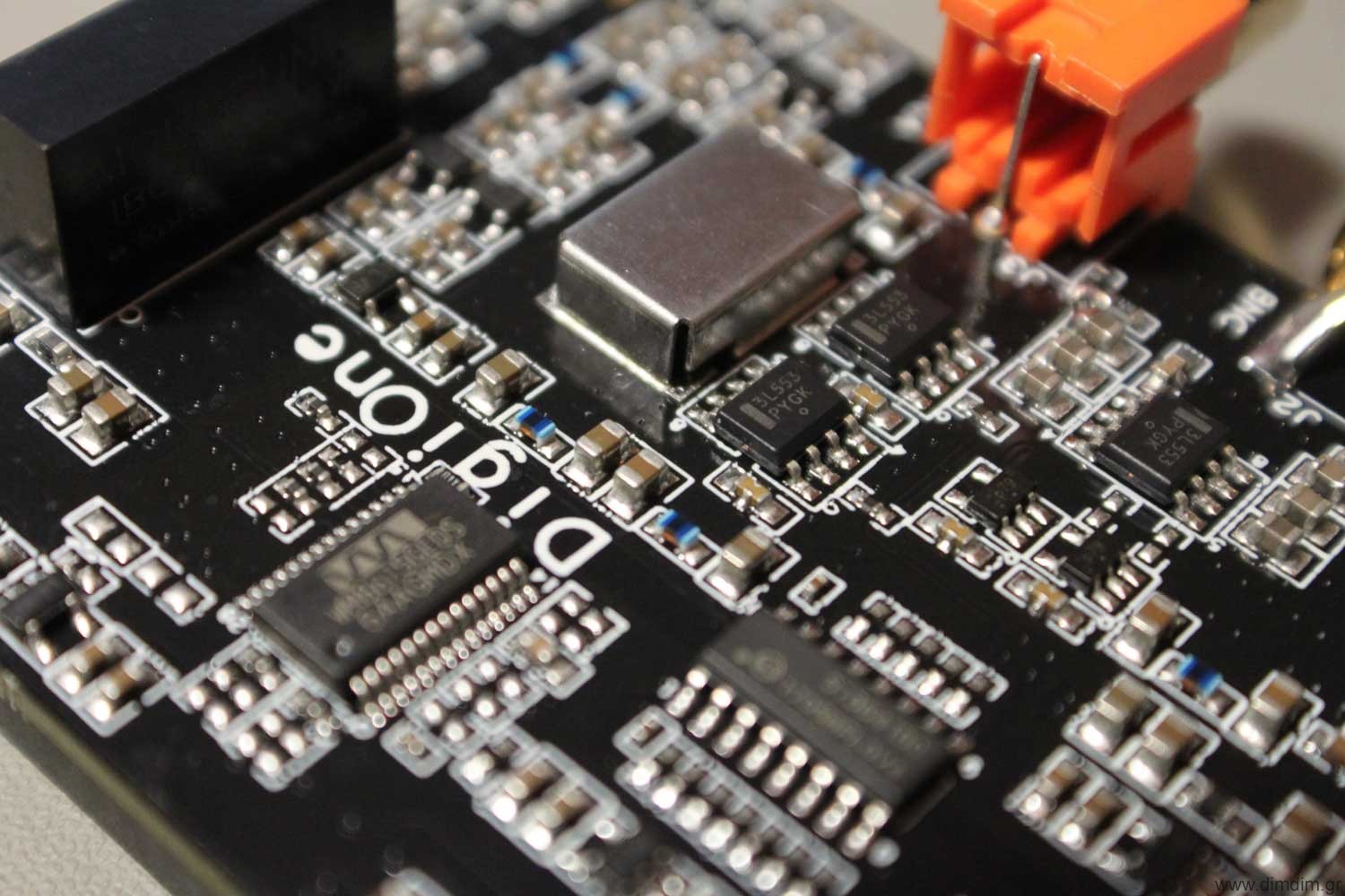
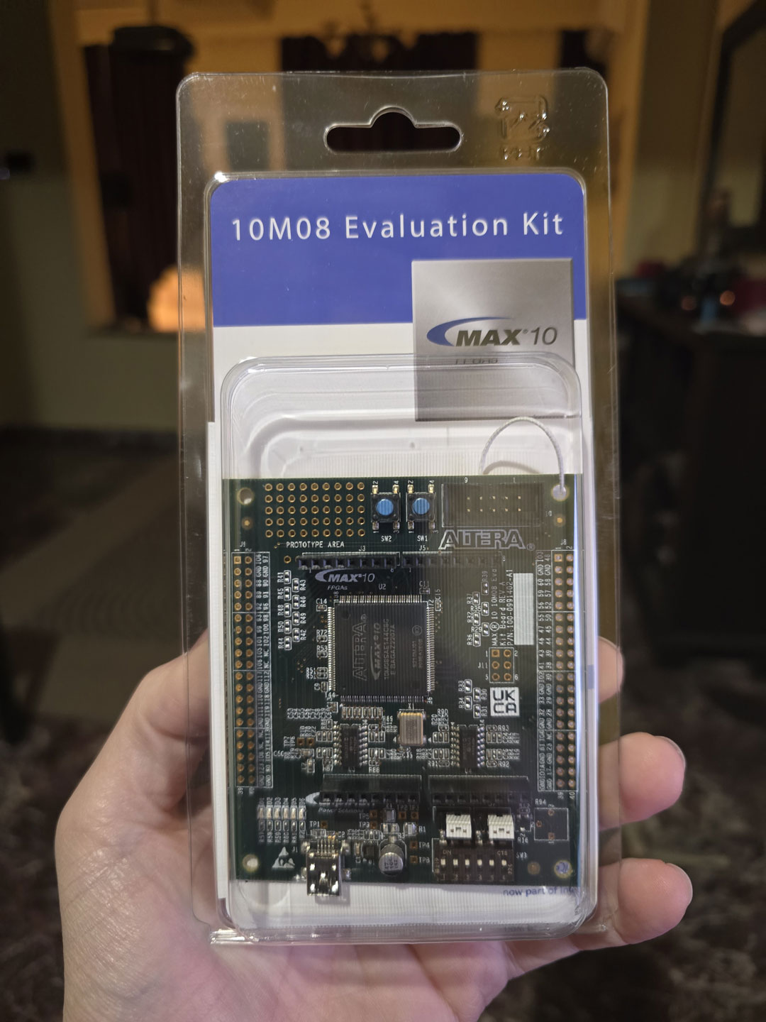
After some deliberation, I ended up picking the Intel / Altera MAX 10. It has variants with plenty of horsepower that come at the human-solderable 144 pin EQFP package. Nice.

Plus, you can get a 10M08 dev board on Mouser for about 60$.

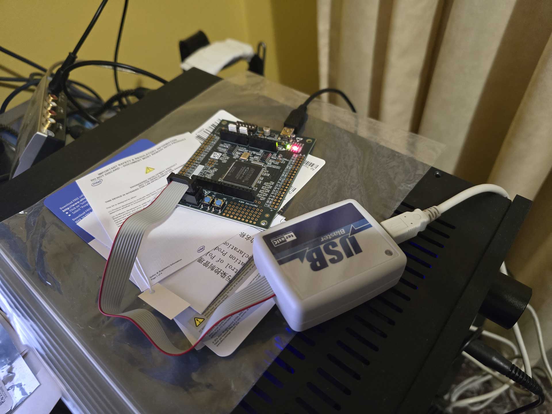
As a matter of fact, the programmer that you will also need (USB Blaster) is in fact slightly more expensive than the dev board itself. You may be tempted to buy a knockoff programmer off of Ebay. Do not buy such a device. It will not work, even though the AIs might tell you otherwise. I got one, tried to get it to work, failed miserably. I asked the AI why I couldn’t get it to work and its reply was something like “oh, you got that one, the Chinese one? Sorry, it’s junk, it will never work, just shell out the 60$ for the proper programmer”.

Sigh.

Anyway, with a working programmer on hand, I proceeded to use Quartus to write my first Verilog “blink” program and upload it to the dev board. The LED began to blink. Awesome.

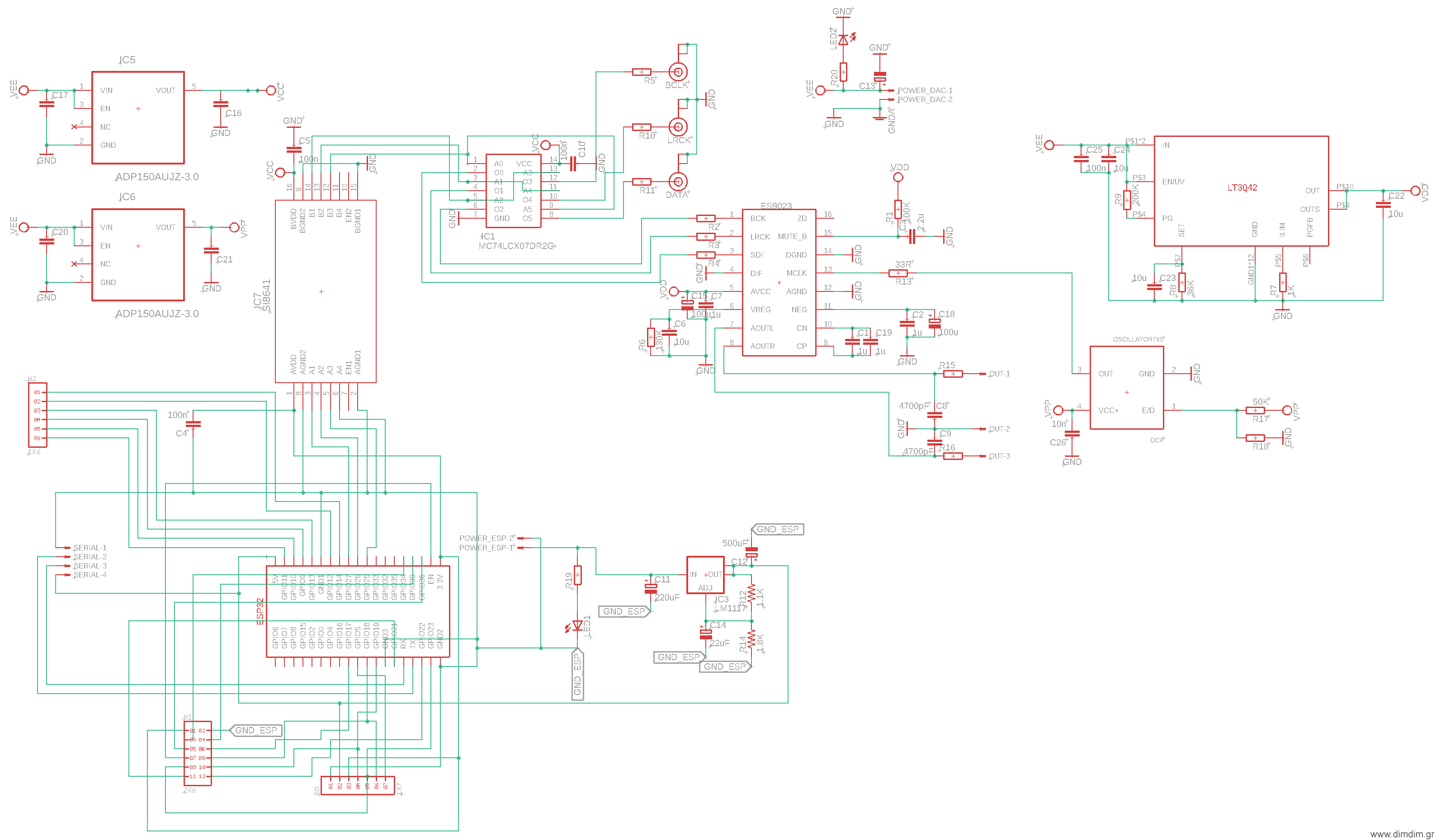
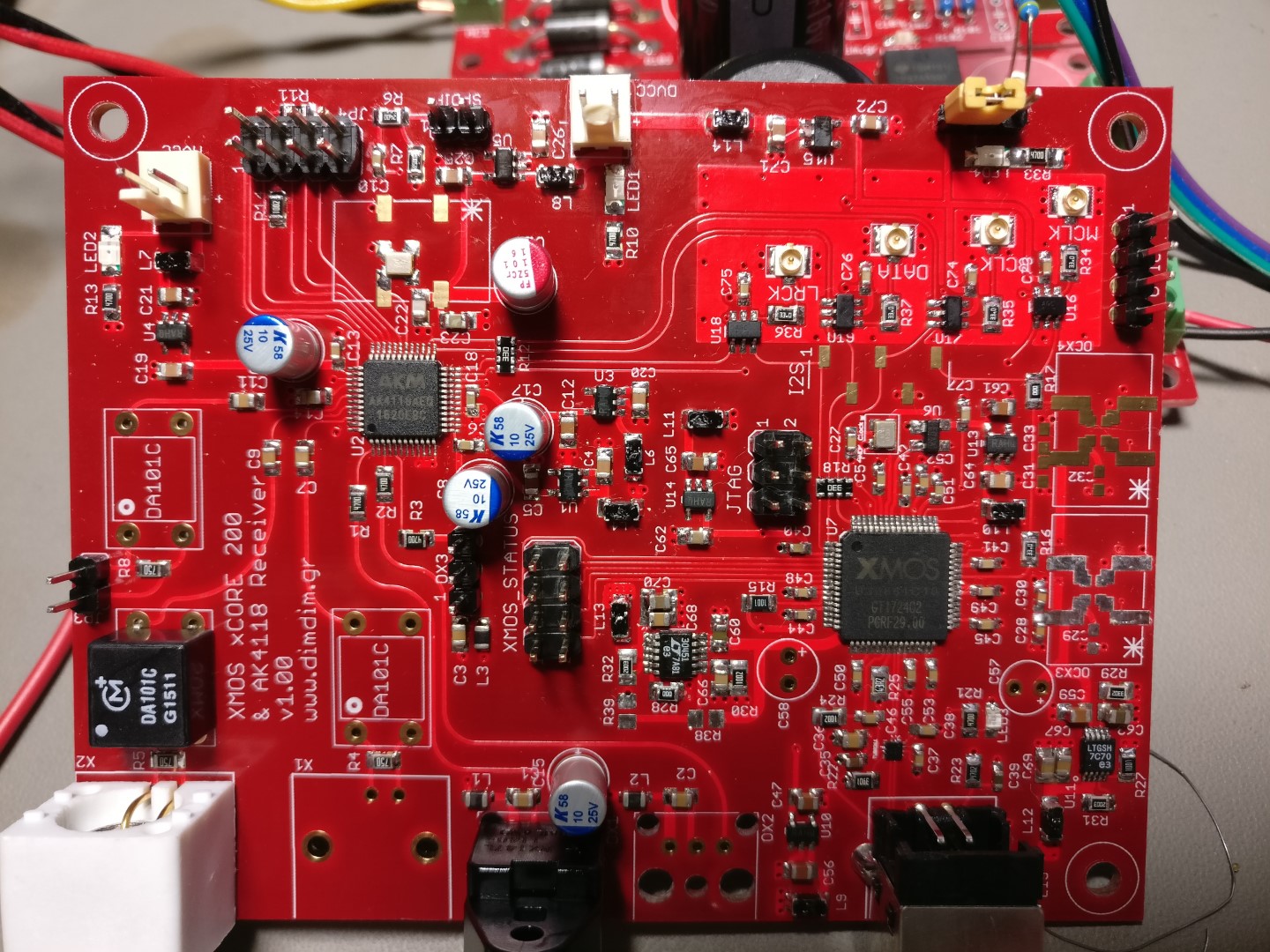
Next up, something useful. With the help of Gemini I proceeded to write (ok, actually copy-paste) a bunch of pieces of code that were supposed to implement an I2S receiver, a Dual Clock FIFO, and an I2S transmitter, just for 44.1KHz sampling rate and 32bits of resolution. It would use PLLs to generate the necessary signals (BCLK, LRCLK, DATA) from the system’s 50MHz clock. Part of the process was struggling with Quartus’ bugs, especially when trying to generate IP and getting garbled screens. The AI helped a lot here, proposing solutions or workarounds to bugs.

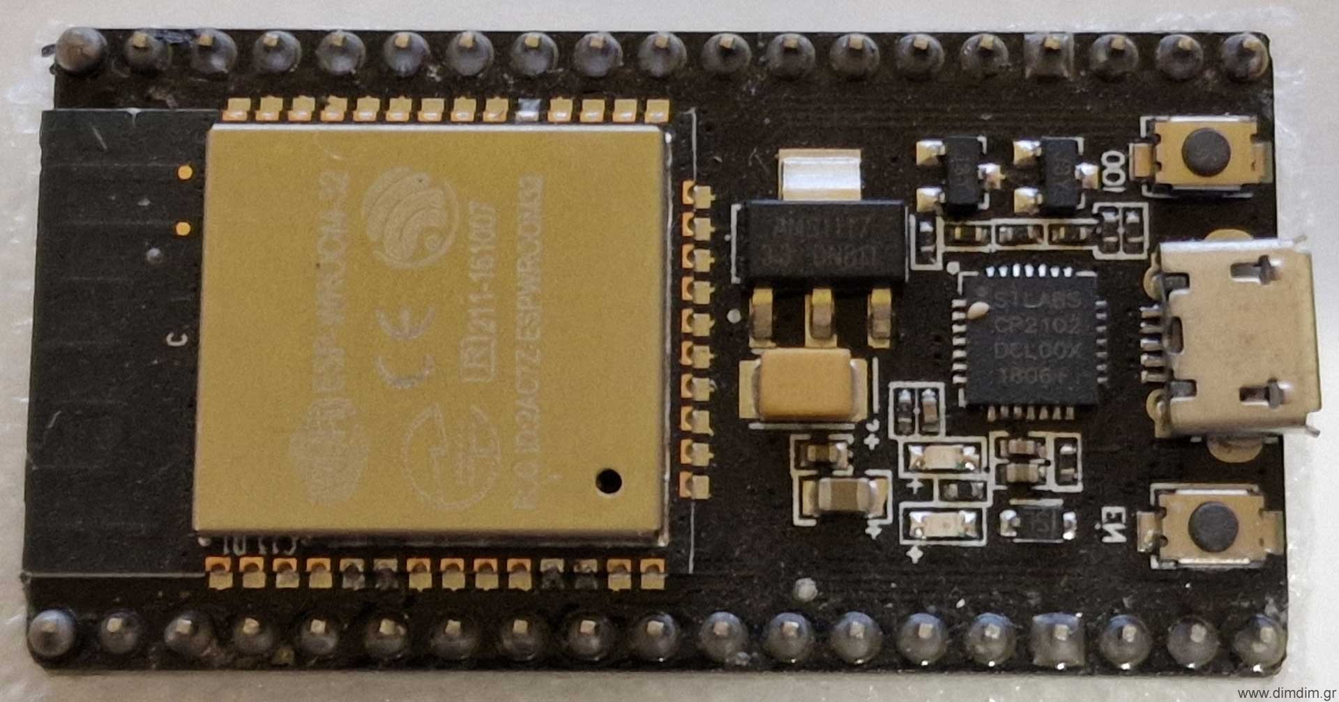
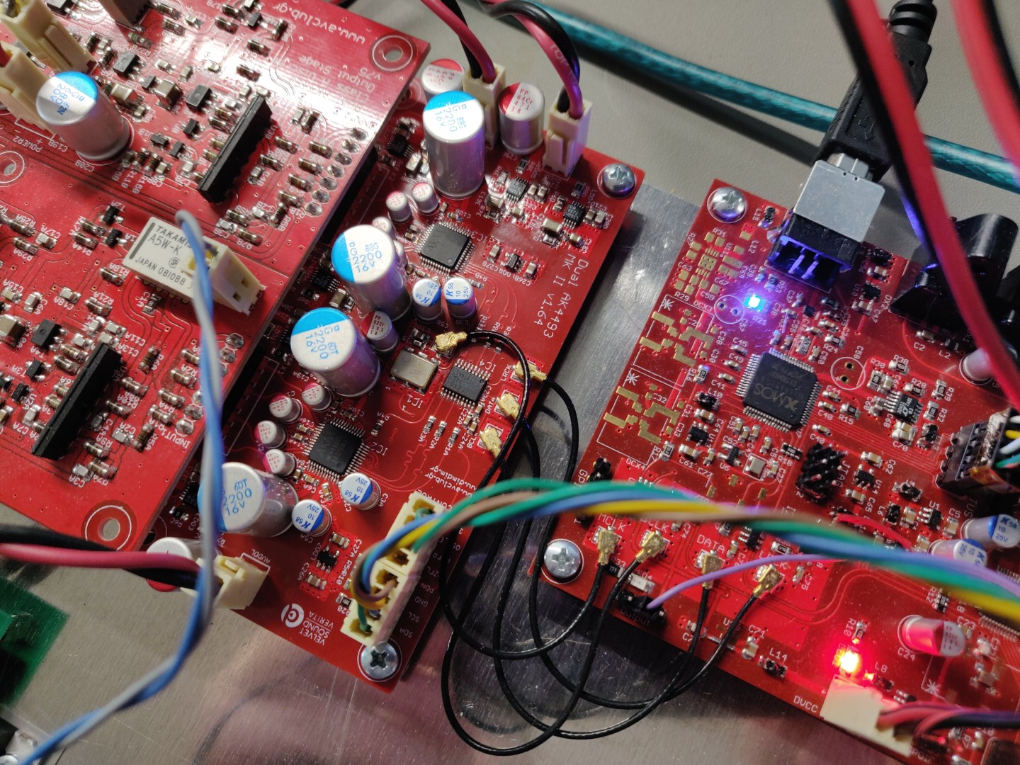
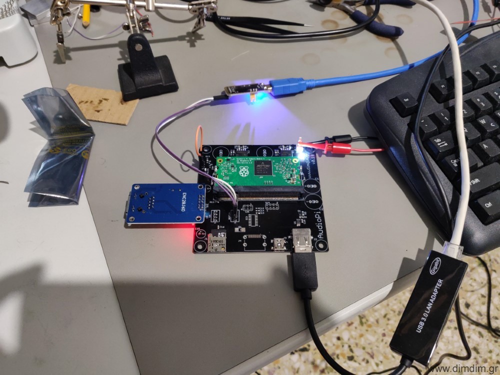
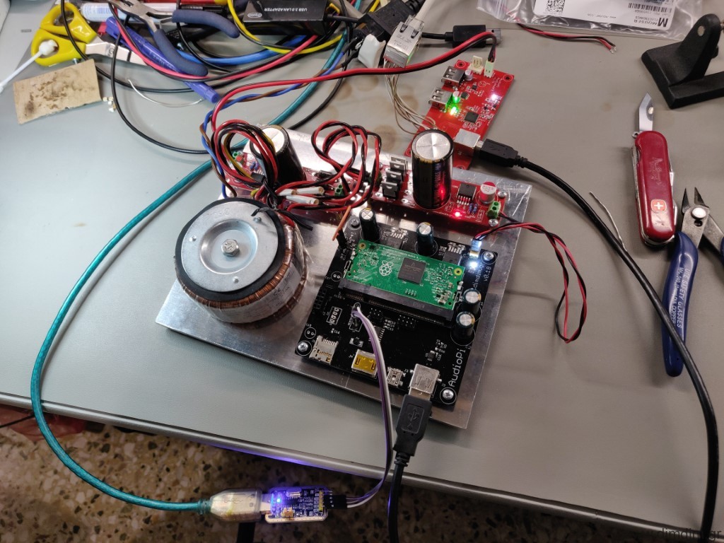
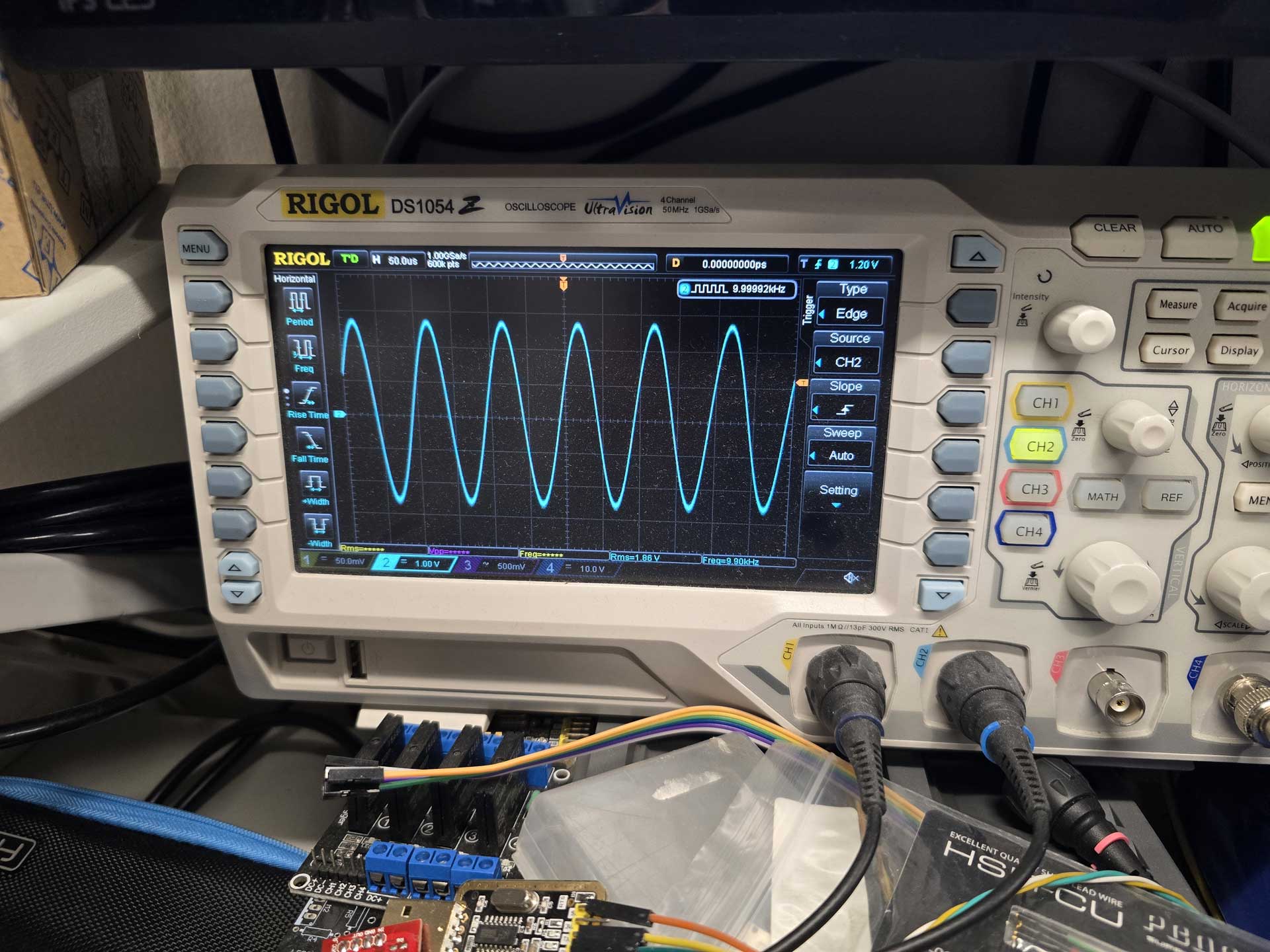
When the test project was built, I hooked up an Amanero as I2S source and an ES9023-based tiny DAC as an I2S receiver. I connected the analog out of the DAC to my oscilloscope and uploaded the code to the FPGA. I played a test file consisting of a 10KHz sine wave and got.. junk on the oscilloscope.

Well, what did I expect? It was a pretty much “blind” attempt at FPGA coding.

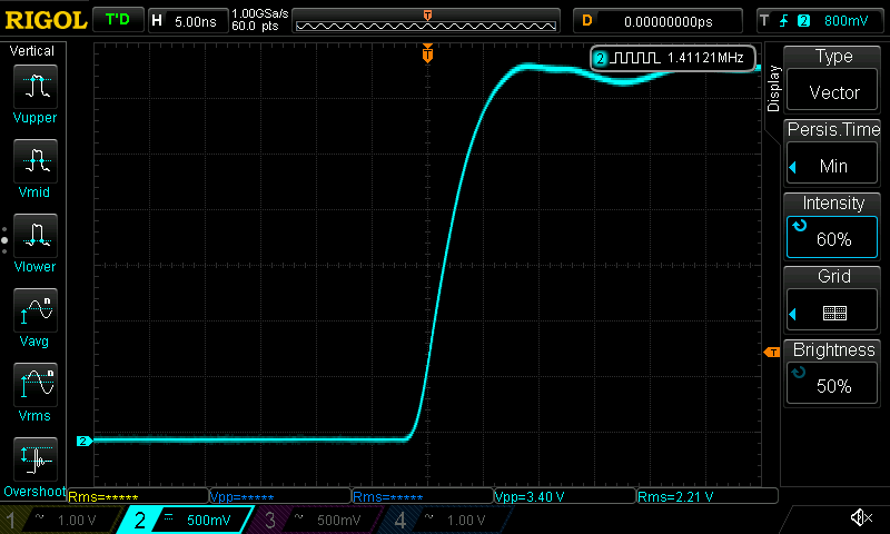
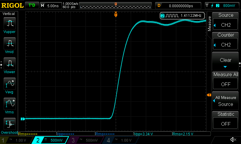
But then ΑΙ magic started to happen. I described to the AI what i was doing and what I was seeing on the oscilloscope and after a few Qs and As it figured out exactly what was happening. It instructed me to make a few changes to the code and lo and behold, I got a clear 10KHz signal on my oscilloscope!

So i had a system that would receive an I2S signal, buffer it in a FIFO, and output it through an I2S transmitter. It was the first and most important step towards implementing what I had in mind, and it was working after a couple of hours of work.

All that without me having to write a single line of Verilog code. So much win.

From then on it was just natural evolution of the project.

I managed to get bit counters working, to recognize the sampling rate of the incoming signals.

I got external MCLK working, so that I could run the output of the FPGA synchronously with the DAC.

I got a bidirectional UART working so that I could see what’s going on in the FPGA and instruct it to do things like change input or tell me the sampling rate, etc.

But not everything worked right away. I got the idea of implementing a PRBS-15 bit perfect test routine so that I can have visual confirmation that the FPGA is not screwing up something in my signal. Gemini 3.1 Pro could not figure out why it didn’t work. Neither could Claude Sonnet 4.6. Neither Claude Opus 4.7. So I gave up on PRBS and switched to a “known pattern recognition” algorithm. That worked straight away and was definitely good enough.

Then I added DSD compatibility with automatic signal type detection.

And a DoP decoder.

And DSD stuck bit protection.

And a real bit depth detector.

And LEDs that show the status of the FIFO buffer, along with Bit Perfectness and DSD Muting.

And multiple I2S inputs.

And an S/PDIF receiver and decoder implemented inside the FPGA.

It also gave great help in creating an SDC (Synopsys Design Constraints) file for the project, which is a must have when you are dealing with high frequency, jitter sensitive signals.

During our conversations it did need reminding of what we had already implemented, due to the AI’s limited context window, but overall it was doing a very decent job.

And there were cases where it hallucinated, causing me to go down the wrong path, wasting time.

But the real test of the AI’s capabilities (and my patience) was when I got to the part of adding a PSRAM chip for extra buffering time.

It was a real challenge. The AI wrote a bunch of routines that managed the communication with the PSRAM over a QSPI bus, the handling and packaging of the data, the pseudo-concurrent reading and writing to the memory, and much much more.

Of course, it didn’t work on the first try.

Or the second.

Or the third.

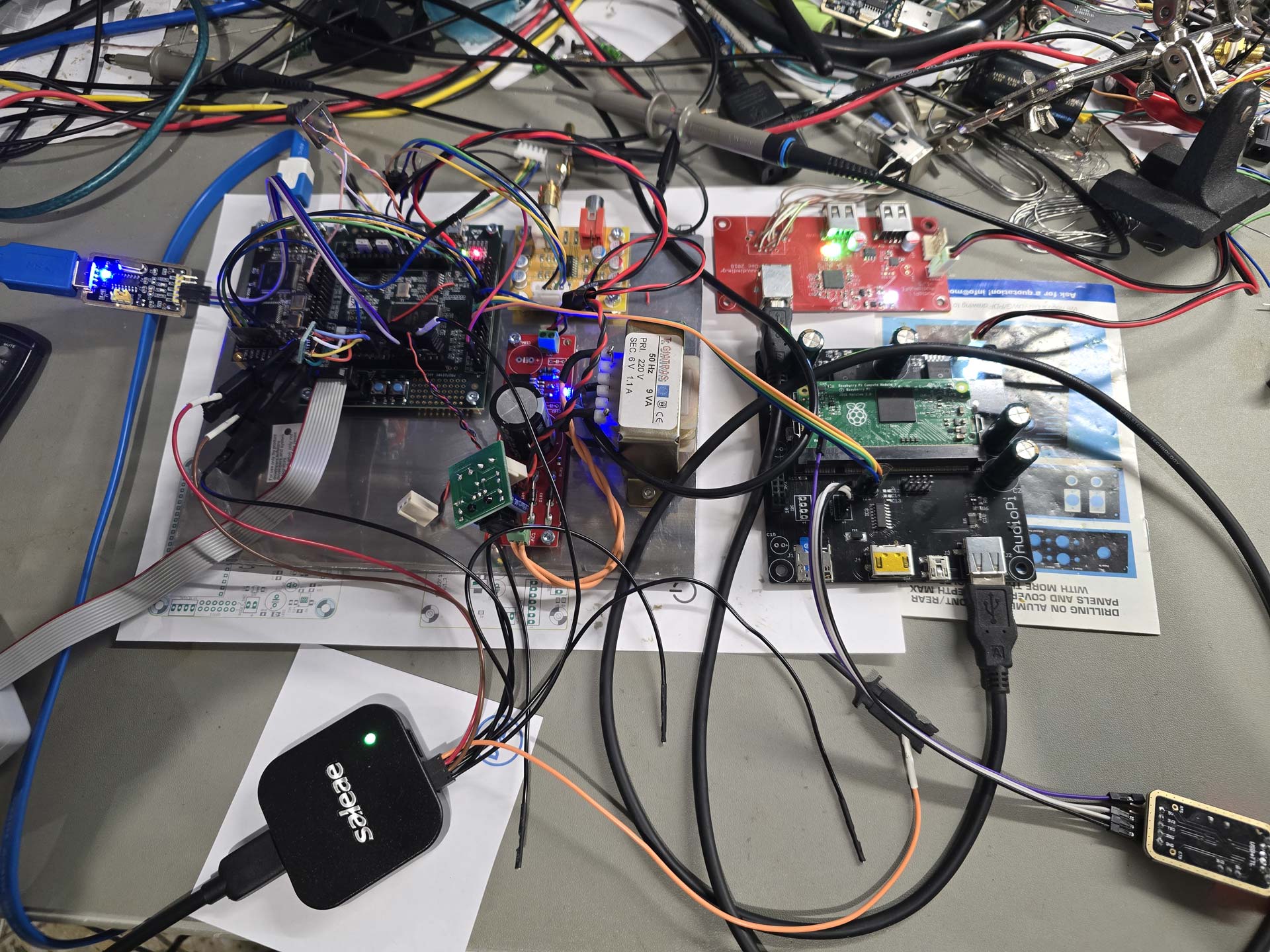
At about that time I realized that looking at a fuzzy oscilloscope screen, describing to the AI what I was seeing and expecting it to figure out what was not working was not going to cut it.

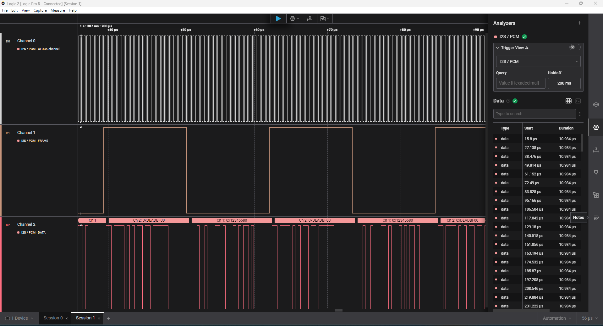
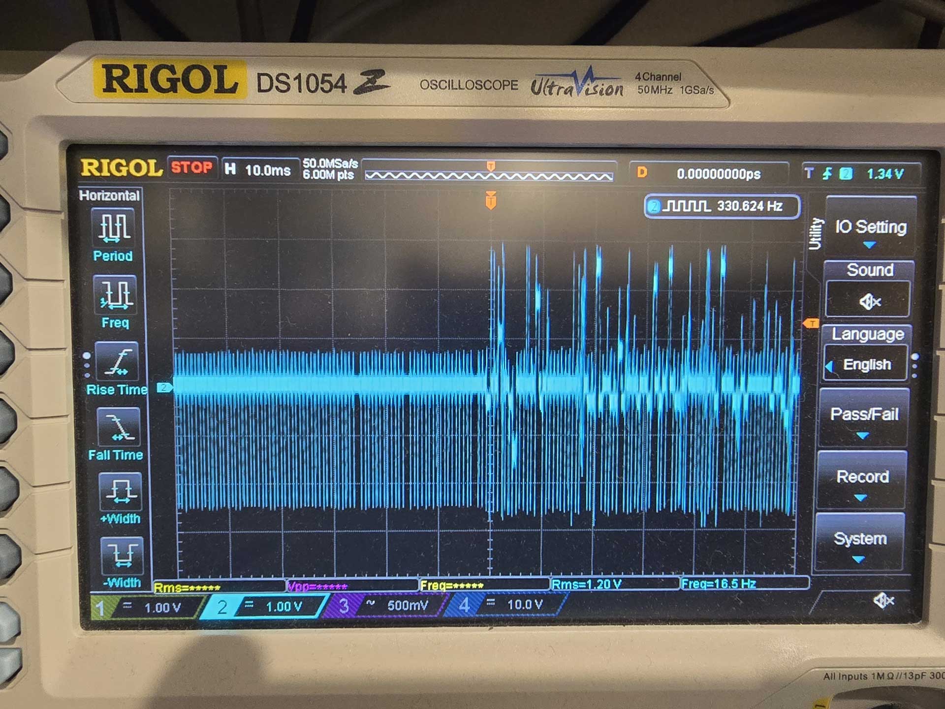
So I asked the AI to break down the FPGA architecture into smaller parts that could be tested individually. It congratulated me for my brilliant idea and did just that. So we wrote routines that checked the data in the PSRAM for corruption, using LEDs for diagnostics, using the UART to get a lot of debugging info, but still we only got so far. In the end I had to break out my Saleae logic analyzer and do some classic troubleshooting, injecting known signals and seeing what the code was doing to them. But that did the trick. Not before long my FPGA was successfully using my PSRAM as a 64Mb buffer, working bit-perfectly.

So this is what I’ve been up to for the last 20 days or so.

It was fascinating to realize exactly what FPGAs are capable of. For example, the realization that the building blocks that I was creating all worked essentially in parallel, and that there was no such thing as “CPU time”, being shared among components, was a revelation. The deterministic nature of these devices. A signal of certain specifications will always be processed at the same speed, no matter how complicated I make the rest of the project. I can simply add modules that “tap” into the same signal and do things, with no consequences to my initial signal processing.

I must say that this was the most fun I have had with a “new technology” for a really long time. It was extremely rewarding to realize that a project of such complexity can indeed be “vibe coded”. Even though I did learn some Verilog in the end. Not because I had to, because I wanted to.

So, can anybody just get an evaluation board and end up with a working FIFO reclocker?

It will depend on your working knowledge of DAC architectures.

You will need to describe to the AI what you need to accomplish, and guide it step by step towards it. But you cannot just tell it to “make for me an FPGA that does FIFO buffering of I2S and DSD signals” and expect it to just do it. If you just give it a single prompt describing the entire thing that you have in mind, however much detail you can provide, it is 100% certain that it will not work, and you will have a nightmare of a time figuring out exactly what is not working.

So it will be a process.

But if you persevere, and you have a logic analyzer on hand, you will eventually succeed, like I did.

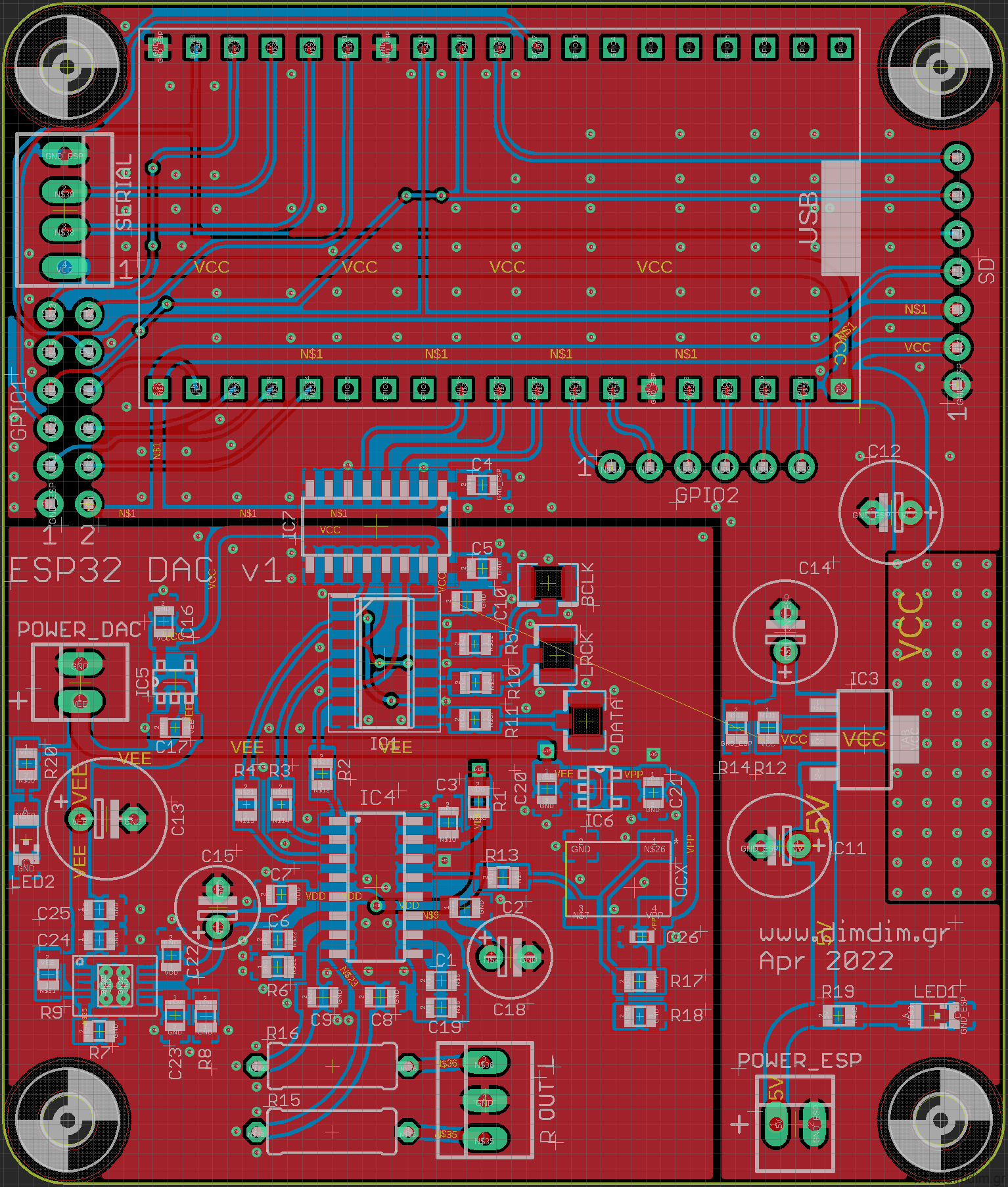
Next step for me will be to design a custom PCB for the FPGA and the necessary reclocking stage that has to follow it.

And while I am waiting for the PCB fab I will tackle the upsampling and digital filtering code.

There is enormous potential here.

PS. Absolutely no AI was used for this writeup. Unlike the FPGA coding.

ESP32-based Internet Radio Streamer

A long time ago I bought an ESP32 module off of Ebay. I can’t really remember what for, but I did.

These things are dirt cheap, costing something like 4-5€ with shipping and feature a 32 bit dual core processor, plenty of flash and RAM and a wireless module supporting both WiFi and Bluetooth. They also sport a lot of GPIO and there is official Arduino support from the manufacturer ( https://github.com/espressif/arduino-esp32 ), so programming them is very easy. In fact, here is a guide to flashing the module with the Arduino IDE.

So the module arrived a couple of months later, in typical China-to-Greece-by-post fashion. By that time I had literally forgotten what I had bought it for. So it then lay there in a drawer for 4 or 5 years until I randomly came across an article that mentioned that it can output I2S! That was news to me, and obviously interesting.

After a brief google search I came across this project: https://how2electronics.com/simple-esp32-internet-web-radio-with-oled-display/ which then led me to this very cute library: https://github.com/schreibfaul1/ESP32-audioI2S

So I entered my favorite internet radio’s URL, plus my WiFi credentials into the code and loaded it to my ESP32 using the Arduino IDE. Surely enough, I saw in my serial port that the ESP32 connected to my WiFi access point and then opened successfully the streaming radio station. I could see on my oscilloscope that it was indeed outputting I2S. Excellent!

Then I hooked up a tiny DAC board that I had lying around (sporting an ES9023 chip – very practical since the ESP32 does not output an MCLK signal), and the thing worked flawlessly on the first try!

So I thought that I should do a carrier board for the ESP32 that would perform the following:

  1. Host the ESP32 board,
  2. Provide regulated power to the ESP32,
  3. Provide headers for serial port (programming), SD card, extra I/O, and perhaps for an LCD,
  4. Do galvanic isolation of the I2S signals,
  5. Provide buffered I2S output for connecting to an outboard DAC board,
  6. Have an on-board DAC with line level outputs.

Since this device would only stream internet radio (a.k.a. “heavily compressed audio”), the on-board DAC did not have to be anything special. So let’s go with the all time classic ES9023.

Let’s also do a relatively good power supply for the critical component (dac chip) but nothing extreme. The rest of the audio-related components can be powered by well respected LP5907 LDOs, while the actual ESP32 can be powered by a run-of-the-mill LM1117.

So this is what I came up with:

Gerbers were generated ( ESP32_DAC_v1_Gerbers (45340 downloads ) ) and an order was put into a well known Chinese board manufacturer.

A couple of weeks later the boards turned up:

And were promptly populated:

Here is the complete Bill of Materials for this board: ESP32_DAC_v1_BoM (53282 downloads )

A suitable power supply was also implemented and integrated into a proper case:

And here is the completed device in action:

This was a pretty simple and relatively low cost project, an ideal way to keep busy for a couple of winter evenings.

Also it is a good way to listen to high fidelity internet radio without needing to keep an entire PC and DAC powered up. So it’s good for the environment.

It would not be difficult to add an LCD that would display the artist and track that is playing.. perhaps sometime in the future.

Soekris dam1021 update

Hi guys, long time no see.

Easter time here, so I have some time to spare, so here it goes.

Update on my DAM build

My Soekris has had a number of upgrades performed to it over the last 2-3 years that I haven’t posted about and it’s about time that I did.

The first upgrade was a switch from Salas BiB 1.1 to an UltraBiB 1.3. I wrote about the upgrade on the official UltraBiB thread:

I was (and still am actually) one of the lucky few that got to beta test Salas’ new baby.

This thing is remarkable.When we swapped it in place of the BiB 1.1 in my Soekris, the improvement was immediately obvious and not subtle. There was a general improvement in clarity and silence, but the biggest improvement (imho) is that the music appeared to have more energy in the lower mid area, where before it was kind of “dry”. This was with Salas’ very first prototype, built with standard (non-boutique) components. The board that I built with audio grade capacitors in the filter bank and MUSE BP caps in the output sounded even better.

I do need to experiment further with different brands of caps (especially in the C2 & C3 positions) but in any case this is an excellent power supply, substantially better than the BiB 1.1, both subjectively (the way it sounds..) as well as objectively (measured performance).

The next upgrade was when I upgraded my firmware to the newer firmware (rev.1.21) that doubles the number of supported filter taps from 2K to 4K. Even the basic / included filters provided a substantial improvement in imaging and detail. Definitely a worthwhile upgrade.

The final upgrade was the design and implementation of my own XMOS-based USB receiver, specifically for the DAM:

The idea was to include just the right mix of features that would make sense for the DAM1021. So, I did include ultra low noise LDOs (LT3045 & LT3042), SDA oscillators, reclocking with a Potato FF, but I skipped galvanic isolation since the DAM already supports it.

The improvement it made in sound quality was remarkable. It’s funny how all digital devices that are supposed to be immune to I2S signal quality turn out to be.. well.. influenced by I2S signal quality. The USB receiver that it replaced was the DIYINHK XMOS receiver that I have used in my DAM, which was pretty decent at the time of purchase. But the newer XMOS family (XUF208) coupled with the ultra low noise LDOs and the reclocking apparently did the trick.

The funny thing is that the prototype I built was actually tested in a good friend’s DAM and has been living there ever since. Someday I’ll build another one for my DAM. For the time being, I’m busy with my AKMs and ESS’.

Update on the DAM board offering.

A few days ago Soren announced Rev. 7 of the DAM1021:

(picture courtesy of soekris.dk)

According to Soren, the new boards will include the following changes / improvements:

1) it use the same FPGA and same uC as usual, so should be able to use same firmware, there are some differences, so new firmware are needed and will autodetect board.

2) The shift registers are now also in the smaller qfn packaging as used on other boards, so I don’t need to stock the tssop types anymore….

3) Output shift registers now running at 1.4M/1.5M sample rate, making FIR2 filter different. Will require new filter file, but plan to use same filter file for both old and new boards, firmware will load filters as needed.

4) The R-2R network is now 24+3+1, ie 24 bit classic R-2R network, 3 bit thermometer network, plus the sign, total 28 bits.

5) Yes, still same Si514 clock, but now in a small package (like I use on other boards), and it drives the shift registers directly, no added jitter by going though the FPGA. People who want to bitch about the Si514, please go elsewhere, we have heard you multiple times….

6) The clock Power supply is separate and use a LP2907 low noise regulator.

7) New vref supplies, like used on the dac2541. For those who want details, yes it use a opamp with transistor buffer, with a polymer output capacitor. Lower vref impedance from DC to Megahertz.

8) Those are powered at +-5.4V from LM317/LM337 pre regulators.

9) Output opamps are opa1678.

10) Power in are now DC only, optimal is +- 9V.

11) The board is mechanical and almost electrical compatible with previous version of the dam1021.

12) J9 is 4 bits user i/o, planning to use it for additional SPDIF inputs.

13) The non isolated serial management port is now TTL levels, not real RS232 levels. So get the right USB to serial adapter….

So quite a few changes, with the most significant being the Si514 having its own regulator (mentioned at a later post in the thread) and driving the shift registers directly. Plus new VREF supplies.. These improvements should be pretty audible.

It looks like the only flavor that will be available will be the dam1021-12.

We’ll see how it will go.

Stop the press: Archphile is back! Codename: “corona”

Archphile used to be the RPi audio distribution of choice for the most hard-core RPi-lovin’ audiophiles around until last June when Michael (tuxx) decided to drop it.

Then in January he hinted to it coming back at some point.

Well, it appears that that moment has come. Head over here for more: https://archphile.org/blog/archphile-119-codename-corona-for-rpi23-and-odroid-c2-is-up/

And not a moment too soon.. My Audio Pi is pretty much ready and it is in desperate need of a proper audio distribution. This should be interesting.

Dual Mono AK4493 DAC (MK II)

Time flies when you’re having fun. Or are just too busy with things, in general.

It’s been two and a half years since I posted about my Dual Mono AK4490 DAC. That DAC has been built and is in use by at least 6 people, other than myself. All of them have been very satisfied with its performance.

But since then quite some water has passed under the bridge.

Among other things, the AK4493 chip came out, and it was just that much different than the AK4490 that I had to update my design to accommodate it.

Feature-wise it was pretty enticing. It looked more like a limited performance version of the AK4497 than an upgraded version of the AK4490. So I had to try it out.

Since I was going to update the PCB design, I thought I might as well improve on as much as I could. So, the new board would:

  • Include a new reclocking solution. I went for the best specc’ed chip out there, the famous Potato Semi PO74G374A. One chip would take care of the all of the I2S lines for both DAC chips.
  • Add a couple of external 1.8V DVDD power supplies.
  • Make some optimization of the LT3042 local regulators’ layout, in order to accommodate larger package capacitors (1206) where it would make most sense.
  • Give access to the zero-detect lines of one of the dac chips. These pins could be used to easily implement auto muting of the output stage.
  • Give access to the Enable pin of the Si570/Si544. The use of this Enable pin will be explained later.

In addition I would use the then new Si544 programmable oscillator, offering improved performance over the Si570. This did not require any changes to the pcb.

This is the updated schematic:

(Right click, Save Image As.. to download it in full resolution)

This is the 4-layer PCB:

And this is the BoM (v1.9) in xls format: Dual AK4493 DAC (main board BoM) (65041 downloads )

The finished board looked like this:

The design consideration, powering scheme and clocking considerations remain the same as with the original design. There is not much sense in repeating the same text here. I will make a few notes though, based on the experience gathered from building, testing and listening to several such DACs.

  1. Reclocking is indeed a good idea, offering both measurable improvement in jitter as well as better sound quality.
  2. The pre-regulators that power this board matter. A lot. Especially the ones for AVDDL & AVDDR. We got the best (audible) results by using a couple of paralleled LT3045s.
  3. In a resolving system, any change in anything makes audible differences. I was particularly surprised to hear how much of a difference having correct (and uniform across my devices / stereo components) electrical phase in my power cords made.

Also, having a properly designed and implemented USB to I2S receiver is very important. Early on I realized that it would be best if I designed my own XMOS-based receiver board, custom tailored to my needs. It would also include some light USB line conditioning and an AK4118-based S/PDIF receiver with 4+2 inputs. I would then standardize my DAC designs with this inputs board in mind, including properly supporting it in my Arduino code.

And so this board came to be:

Describing in detail this board is beyond the scope of this post, but suffice it to say, building it is not for beginners. Plus you will need XMOS’ xTAG programmer to burn firmware into the XMOS chip. If anybody is feeling particularly adventurous, drop me a line and I’ll see if I have any PCBs left.

Now, regarding the Arduino code needed to control this board(s), it is not very different than that used to control the AK4490s. The main differences are:

  • It has been adapted to enable the AK4493s’ PCM/DSD auto detection feature
  • It has support for all of the AK4493’s digital filters
  • It has support for triggering a muting relay
  • It now supports the Si544 instead of the Si570
  • It offers full compatibility with my XMOS / SPDIF board.

There are a number of to-do’s though, such as displaying the bit depth of the incoming PCM signal (from the USB port), plus more information on the incoming DSD stream (such as whether it is in DoP or Native format).

The hardware of the controller is the same that was used with the Dual Mono AK4490 DAC.

In this download I am including the modified versions of the libraries (as mentioned in the above linked post) as well as the necessary font files. Be sure to extract the contents of “Libraries (place in Libraries folder)” to your Arduino IDE’s “libraries” folder.

Download it here: aKduino v3 (405097 downloads )

Regarding the output stage, it is the same design that was used for the AK4490 DAC. However its output level is slightly lower than that of the AK4490 board since the AK4493’s VREF voltage is limited to 5.25V, compared to about 7V of the AK4490. This difference in volume is easy to compensate for by changing a few resistors on the output stage.

Here is a pic of the 3 boards in action:At the time of this writing there have been built 4 DACs based on this updated DAC design PCB.

If anybody is interested in building this DAC drop me a line. I have a few spare boards lying around.

Allo DigiOne S/PDIF HAT

First off, I’m ashamed to admit that I had this little gem in my possession for about 2 years before I finally got the chance to put it through its paces.

After all, it’s just a s/pdif output device for a Raspberry Pi, right? I mean, it’s just s/pdif, how good could it be?

It turns out it can be pretty damned good! But I’m getting ahead of myself.. Let’s start at the beginning.

The DigiOne is a HAT compatible with most if not all RPis and supported by most if not all audio distributions. It is intended to be plugged-in directly on top of the RPi, with no need for an isolator HAT. Plus, it is designed to be powered by the RPi via the GPIO header, so no need (or provision) for an external power source.

The DigiOne utilizes a WM8805 to convert the RPi’s I2S signal into s/pdif. The WM8805 is run in master mode, so as to minimize jitter due to the RPi’s problematic I2S clocking scheme. The WM8805 is clocked by the same oscillators that are used to reclock the s/pdif signal.

The WM8805’s s/pdif output goes through an Si8641 150MHz galvanic isolator and is passed to the “clean” side of the board.

There the signal is reclocked by a high quality flip-flop clocked by high quality NDK oscillators (housed inside a metal box, used for shielding against EMI/RFI). There exist two oscillators, one for the 44.1K family and one for the 48K family of sampling rates. The output of the oscillators is put through NB3L553s for buffering and isolation.

The entire isolated part of the board is powered by a DC-to-DC converter that offers galvanic isolation. Following this converter there exist a large number of LDO regulators and filter components. An LT3042 regulator is used to power one of the most critical parts of the circuit: the flip-flops that do the final reclocking.

So, very solid engineering all around. But how well does it sound?

The answer is, surprisingly well for the money.

My RPi stack included an RPi 3 with the DigiOne, powered by Salas’ new L-Adapter power supply and running Archphile. The music was coming from my NAS. No audiophile ethernet switches were employed. 😛
Pitted against that I had my Logitech Squeezebox Touch running the EDO plugin for up to 192K s/pdif from its coax output and my relatively pricey Pioneer DV-LX50 Universal Player (using its coax s/pdif output).

The music used was Dire Straits’ SACD album (having selected its CD (and not SACD) layer) which was also accurately ripped to my NAS.

Output from the s/pdif transports went into an AK4118-based s/pdif receiver of my own design which in turn feeds my dual mono AK4493 DAC. The DAC’s output goes through a Salas DCG3 preamp into my Hypex amp.

First up was the Pioneer. It had been a while since I had listened to it through its s/pdif output so I was in for a bit of a shock. Its output sounded coarse, strained, tiring. For a moment I thought that it was due to the SACD’s mastering (the CD layers of SACDs are rumored to be mastered intentionally bad so as to give the impression that the SACD layers sound even better than they actually do), but that changed when I switched to the Squeezebox. Things got noticeably better, actually listenable. Not exactly close to what I had been accustomed to using the Squeezebox’s USB port, but closer.
Then I switched to the DigiOne. Wow! All of the “coldness” of the music was gone, the stage gained depth and width, the music became more detailed and lifelike. This was definitely a step up.

I would dare say that this s/pdif setup came in fact close in SQ to my USB setup. This was a very pleasant surprise.

Now I need to do some A-B testing between the DigiOne and the USB output of the RPi. So to-be-continued..

The Raspberry Pi 4 Model B: Game changer for audio?

About a month ago the Raspberry Pi 4 was announced, pretty much blind-sighting everybody.

For the last (many) years, since the announcement of the RPi 2, we had been used to relatively minor incremental upgrades every time a new RPi came out.

Usually the new processor was a bit faster, we got WiFi and BT, then better WiFi, then faster (almost) GbE network, etc. But until now, all of these connectivity options had to be accommodated by a single USB 2.0 port on the SoC.

But this year everything changed. We got a new SoC (the BCM2711), one that finally supported an RGMII interface for a true GbE port, plus a PCI Express port that is used to give USB 3.0 & 2.0 connectivity at useful speeds.

We also got more processing speed and more RAM options, up to 4GB of fast LPDDR4 memory, dual HDMI outputs, etc.

So, all of the above specs mean that the RPi is definitely faster and more capable than ever as a desktop replacement. But is it indeed a better audio streamer for us audiophiles?

For starters, it’s been almost a month since its announcement and availability (I got my unit delivered just 3 days after its announcement) and AFAIK the well-known audio distributions do not yet support it.

Then there is the increased system complexity and power consumption that comes with the new architecture. More power consumption and more ICs usually mean more noise. More noise is never good news for audio.

So I had to do some testing. The idea was to compare the RPi 3 that I had for a couple of years now to the RPi 4.

To keep the playing field as level as possible both of them were running the exact same software (Raspbian Buster Lite, since ATM that is pretty much the only OS that supports both of the platforms) with MPD loaded and were powered by the same (excellent) Salas L-Adapter power supply.

Connection to my DAC (DIY dual AK4493, very detailed) was through USB 2.0.

The music streamed from a NAS box over Ethernet.

I had a friend over in order to at least try to have a bigger sample size (of ears).

The music used was a handful of tracks that we always use for such comparisons (well known material).

We listened using the RPi3, then shut it down and booted up the RPi4, listening to the same material.

Much to our surprise, we actually preferred the sound of the RPi3!

The RPi4’s presentation had something of a “fatiguing” effect. The sound was a bit more “coarse” that that of the RPi3.

We are not talking about big differences here, but they were there. Note that my system is pretty resolving, every change to any component is audible, so YMMV.

I’m not saying that my (our) results are 100% conclusive, but in any case it seems like I’ll be going ahead with my “Audio Pi” project after all (I was considering waiting for the Compute Module 4 to come out).

An “Audio Grade” Raspberry Pi

Not much free time these days so updates have been slow.. but I have a lot of interesting stuff cooking in the back burner.

One of them is an audio grade RPi.

Essentially it will be a Compute Module 3 on a mainboard loaded with ultra low noise linear power supplies and some necessary peripherals.

The idea came to me quite some time ago but it wasn’t until last November that I decided to actually go ahead with it.

The proof-of-concept PCBs for the mainboard were done by December.

It appears that even the PoC board, with average quality power supplies, has a cleaner I2S output compared to a standard RPi3 powered by an equivalent linear power supply:

RPi 3:

Audio grade Pi:

The next part was the PoC board for the USB Hub & Ethernet controller. That took a bit more time and a 4-layer PCB with numerous 0402 sized components but it too ended up just fine (with the exception of a bad RJ45 footprint..).

So now I have a fully functioning set of boards with average quality power supplies that already performs better than my Squeezebox Touch as a USB transport.

Next step is to design a single board integrating all of the components plus ultra high quality power supplies.

That will probably be a summer project..